Combining two or several functionalities into a single metadevice is of significant importance and attracts growing interest in recent years. Multifunctional metadevices perform different functions depending on operation wavelength and the polarization state of optical waves. According to their layer structure, multifunctional metadevices can be usually classified into two types: single-layer type and multilayer type.
Generally, multilayer-based multifunctional metadevices have advantage over their single-layer counterparts in the diversity of functionality. However, the functionalities are usually achieved based on the interaction or coupling effect between the constituent upper and lower metasurface layers, which will hinder independent and flexible design for multilayer metadevices, not only complicating design process but also increasing fabrication difficulty and cost. In addition, many multifunctional devices can only work in pure reflection or transmission mode, not making good use of the full space. Moreover, most previously reported dual-wavelength multifunctional metadevices have lower wavelength contrast-ratio with operation wavelengths located in the same electromagnetic waveband, such as the near-infrared range, Terahertz band, or millimeter regime.

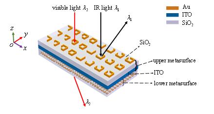
Figure 1. Schematic of the dual-wavelength multifunctional metadevice
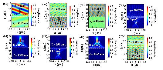
To solve the above problems, Professor Lirong Huang and her Master student Jing Luan, who are from Wuhan National Laboratory for Optoelectronics, Huazhong University of Science and Technology, propose a kind of dual-wavelength multifunctional metadevice, whose structure are shown in Fig. (1). Benefiting from the unique wavelength-selective reflection and transmission of indium-tin-oxide (ITO) layer, the upper metasurface capable of reflective deflection/focusing at 2365 nm and the lower metasurface for transmissive deflection/focusing at 650 nm can be flexibly combined into four different dual-wavelength multifunctional metadevices as shown in Fig. (2), without the need to re-design or re-optimize their structural parameters, which offers a straight-forward and flexible way in the design of multi-wavelength multifunctional metadevices and photonic integrated devices.

Figure 2. (a1) Reflected and (a2) transmitted electric fields at λ1 and λ2 of metadevice 1;
(b1) Reflected and (b2) transmitted electric fields at λ1 and λ2 of metadevice 2;
(c1) Reflected and (c2) transmitted electric fields at λ1 and λ2 of metadevice 3;
(d1) Reflected and (d2) transmitted electric fields at λ1 and λ2 of metadevice 4.
This work was published as an academic paper in journal Scientific Reports (DOI 10.1039/c8nr03564d) of Nature Publishing Group.
This work was supported by the National Natural Science Foundation of China (No. 61675074 and 61805078).