The research work titled “Efficient and large-area all vacuum-deposited perovskite light-emitting diodes via spatial confinement” from Prof. Jiang Tang's group is online in Nature Communications. The manuscript is available athttps://doi.org/10.1038/s41467-021-25093-6
Introduction
The ubiquity of display technology in our day-to-day lives brings a trillion-dollar market worldwide.The recently emerged perovskite light-emitting diodes (PeLEDs) have attracted numerous interests in both academic and industrial fields, due to their high efficiency, narrow emission linewidth as well as low costs of material and fabrication. Specifically, the CIE coordinates of PeLEDs could reach 140% of the NTSC standard, which is much wider than those of industrially dominant organic light-emitting diodes (OLEDs) technologies. Recently, PeLEDs have achieved an external quantum efficiency (EQE) greater than 20%, comparable with that of the best-performing OLEDs, representing an encouraging step towards the practical application of PeLEDs for next-generation display technologies.
However, the current efficient PeLEDs arefabricated by solution-processed methods, such as spin-coating and blading-coating, which aredifficult to integrate red, green, and blue perovskite pixels on the pre-pixelated TFT panels with high resolution.Thermal evaporation,widely used in the semiconductor industrydue to its remarkable scalability and reproducibility, can easily achieve side-by-side three-color perovskite patterns through sequent deposition with the assistance of fine metal masks, which resemble that of OLEDs. Therefore, thermal evaporation is one rational strategy to manufacture efficient and large-area patterned PeLEDs toward next-generation display technologies.
Experiments and results
This work reports the development of efficient and large-area PeLEDs based on vacuum-deposited Cs-Pb-Br films via spatial confinement. By incorporating zero-dimensional (0D) structural Cs4PbBr6into CsPbBr3film, the 3D connection of [PbBr6]4-octahedra is partially broken, forming Cs4PbBr6/CsPbBr3core-shell structure. The electrons and holes formed in CsPbBr3are spatially confined by Cs4PbBr6. As expected, a blue shift in photoluminescence (PL) wavelength from 516 nm to 480 nm is observed as the CsBr/PbBr2molar ratio increased from 1.24 to 2.28. the carrier recombination dynamics of thermally evaporated Cs-Pb-Br films are further investigated via femtosecond-transient absorption and found that perovskite film of CsBr/PbBr2=1.56 shows enhanced radiative recombination rate and suppressed nonradiative recombination rate compared to that of CsBr/PbBr2=1.24. Based on an optimal molar ratio of CsBr/PbBr2, the most efficient thermally evaporated PeLED was constructed with a record EQE of 8.0%.
Moreover, benefitting from the excellent uniformity and scalability of the thermal evaporation successfully fabricated large-area (10 cm×9 cm) and patterned perovskite films (the diameter of pixels is ~100 μm), emphasizing the great superiority of our thermal evaporation process. More importantly, a 7.1% EQE for the 40.2 cm2device was achieved, representing one of the most efficient large-area PeLEDs. This work represents one important step to bring PeLEDs from the laboratory towards commercial display panels.
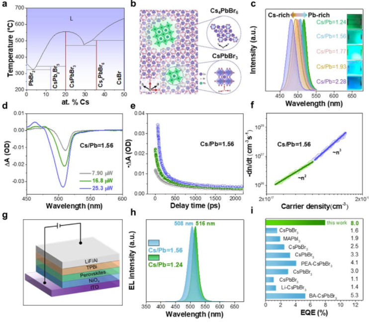
Figure 1. Efficient thermally evaporated Cs-Pb-Br LEDs.(a)The phase diagram of CsBr-PbBr2binary system. (b) The schematic diagram of CsPbBr3embedded in the Cs4PbBr6matrix, which indicates the 3D[PbBr6]4-of CsPbBr3is separated by 0D [PbBr6]4-of Cs4PbBr6. (c) Manipulation of spatial confinement through optimizing the Cs/Pb ratios. (d-f) The carrier recombination dynamics of thermally evaporated Cs/Pb=1.56 film. (g)The diagram of PeLED structure. (h) The normalized electroluminescence spectra. (i) The EQE summary of thermally evaporated PeLEDs so far reported.
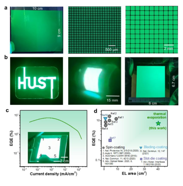
Figure 2.The potential of thermally evaporated PeLED for display application.(a)PL image of 90 cm2andpatternedperovskite films. (b) EL photo of PeLEDs with a “HUST” pattern,flexible substrate, and 40.2 cm2area, respectively. (c) EQE-current density curve of large-area PeLED (40.2cm2). (d) The reported EQE of large-area PeLEDs (exceed 1 cm2) based on various deposition strategies.
Acknowledgments
This work was financially supported by the National Natural Science Foundation of China (61725401, 62050039, 5171101030, 51761145048, 62004075, 62005089), Fund for Innovative Research Groups of the Natural Science Foundation of Hubei Province (2020CFA034), the National Key R&D Program of China (2016YFB0700702, and 2016YFB0201204), the Post-Doctoral Innovative Talent Support Program (BX20200142), China Postdoctoral Science Foundation (2020M682413, 2019M662624), and the Graduates’ Innovation Fund of Huazhong University of Science and Technology (No. 2021yjscxcy036). The authors from HUST thank the Analytical and Testing Center of HUST and the facility support of the State Key Laboratory of Materials Processing and Die & Mould Technology. We also thank Prof. Tianyou Zhai from HUST for providing access to conducting optical characterization.