Filters are one of the main functional devices of integrated photonics technology, which have important applications in various optical fields such as spectral analysis, nonlinear optical wavelength conversion, and wavelength-division multiplexing (WDM). For instance, optical quantum computing and communication use a single photon with low light field intensity as the basic quantum, which thus requires a filter device to effectively extract weak single-photon signals from noise.All kinds of single-photon sources basically produce a single photon by using strong pump light. So, as to prevent the sensitive single-photon detector from being affected by the pump light, high extinction ratio filters are necessarily indispensable. On the other hand, for reducing the loss of a single photon, filters used in the integrated optical quantum chip need to achieve a lower insertion loss compared to the classical optics.
Mach–Zehnder interferometer (MZI) devices have certain filtering capabilities, and many high extinction ratio filter solutions based on cascaded MZI have been proposed. However, the passband bandwidth of the MZI unit device is relatively wide, and the size of the multi-unit cascade is too large, so there are many limitations in practical applications. The integrated photonic resonant device, such as a microring, is a natural narrow-band filter. However, the extinction ratio of a single resonant device is generally not high enough, and multiple devices need to be coupled to improve the performance. Although a single microring is more compact than the MZI structure, it still covers a larger size in the case of high-order connection. In order to cope with the deviation caused by the manufacturing process and make each resonator work in an aligned wavelength, each resonant unit of these filters needs to be assisted by active tuning, which not only further increases the size, but also brings additional energy consumption and difficulty in control and thermal crosstalk.
Professor Jianji Dong from Wuhan National Laboratory for Optoelectronics of Huazhong University of Science and Technology and Professor Yunhong Ding from Technical University of Denmark proposed and demonstrated an optical filter based on high-order coupled nanobeam resonators.
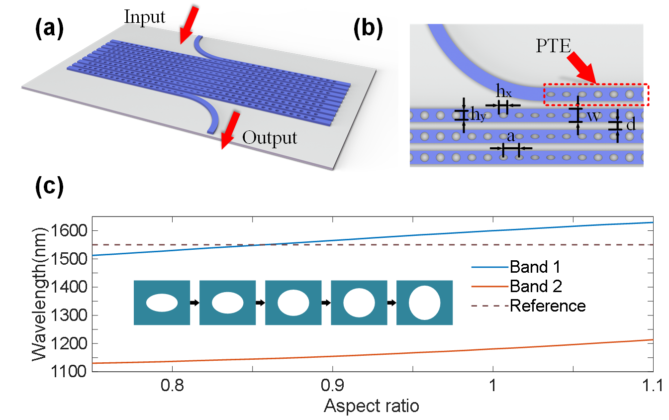
Nanobeam is a one-dimensional photonic crystal resonator with its size similar to a waveguide. Periodic holes are etched along the direction of the beam and defects are introduced in the middle. The light field is confined to the defect, thereby forming a resonant mode. The basic unit of the filter is a high quality (Q) factor nanobeam resonator.Because the nanobeams are shaped like an ordinary waveguide, the order of nanobeams can be effectively increased while keeping the overall size very small when they are tightly arranged in the lateral direction (Fig. 1). As a consequence, the process deviation between nanobeams is minimized, so it is no longer necessary to individually tune and calibrate each resonator like a high-order microring structure, which greatly reduces the structural complexity and footprint.
This research has realized an integrated photonic filter with high extinction ratio and low loss, which provides outstanding performance and extremely small size. The high-order nanobeam resonator filter has an extremely compact size of only about20µm×10µmand a simple structure that does not require active tuning and calibration of each resonator unit. It achieves an extinction ratio as high as 70 dB and an insertion loss as low as 1 dB. The device has a very wide stop band and is not limited by free spectral range (FSR) (Fig. 2). Based on the enhancement effect of the semi-symmetrical partial transmission element (PTE) structure, the nanobeam resonant cavity has broken the bottleneck of transmission efficiency and shown great capabilities. This work can play an important role in a variety of on-chip high extinction ratio filtering applications and has the potential to be used in single-photon source filtering applications in integrated optical quantum platforms.

Fig. 1.(a) Schematic of the proposed CROW nanobeam filter. (b) Partial view and main parameters. (c) Photonic band gap of tapered etching holes.

Fig. 2.Scanning electron microscope (SEM) image of (a) Fano resonance enhanced ninth-order nanobeam filter, (b) coupling area. (c) Schematic of the experimental setup. (d) Transmission spectrum of the actual device. TLS, tunable laser source; PC, polarization controller; DUT, device under test; OSA, optical spectrum analyzer.
Relevant research results were recently published in Optics Letters and selected as Editors’ pick. The work was supported by the National Natural Science Foundation of China(62075075, 61805090).
Full text can be viewed by:https://doi.org/10.1364/OL.433850
[1] Z. Cheng, J. Zhang, J. Dong, and Y. Ding, "Compact high-contrast silicon optical filter using all-passive and CROW Fano nanobeam resonators," Opt. Lett. 46, 3873-3876 (2021).