Recently, in photonic integrated platform, two-dimensional materials such as graphene, black phosphorous (BP) and transition metal dichalcogenides (TMDs) can meet the requirements of future large-scale photonic integrated circuits in terms of high-speed communication and low power consumption. Two-dimensional materials have the properties of ultra-high carrier mobility, strong light-matter interaction, and interlayer Van der Waals force combination, which can be combined with integrated optics to realize high-speed, high-efficiency, and easy-fabrication optoelectronic devices. At present, two-dimensional materials are widely used in laser sources, optical modulators and photodetectors of integrated platforms.

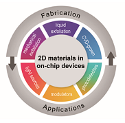
Figure 1. Fabrication methods and applications of on-chip two-dimensional material optical devices.
The article first introduces the synthesis, transferring and processing methods of two-dimensional materials. Then, it summarizes the experimental and theoretical novel research results of light sources, modulators and photodetectors based on two-dimensional materials. Finally, it discusses the design and integration methods of two-dimensional material optical devices and analyzes the challenges in fabrication. This article summarizes the fabrication methods and applications of on-chip two-dimensional material optical devices, as shown in Figure 1. Compared with other similar reviews that have been published, the main differences are as follows:
1. This article systematic summaries the synthesis methods such as exfoliation and growth techniques, transfer methods, and patterning methods of two-dimensional materials. The typical cases are listed to illustrate how to choose suitable processing methods in practical applications.
2. To meet the demand of large-capacity telecommunication in the future, in integrated optics, the fabrication methods and related applications of on-chip active devices, including light sources, modulators and photodetectors, are discussed based on integrated platforms.
3. The basic principles of various on-chip two-dimensional material-based optical devices are introduced in detail, and the novel research results of waveguide-type devices are mainly discussed.
4. This article summarizes various typical two-dimensional material-based optical device structures, listing and analyzing the existing optical structures that enhance the light-material interaction of two-dimensional materials.
Professor Dong Jianji from Wuhan National Laboratory for Optoelectronics of Huazhong University of Science and Technology and Professor Zhang Han from Shenzhen University conducted cooperative research, focusing on the fabrication and application of graphene, TMD, MXene, and BP in high-speed optical communications. The mechanism of waveguide-based two-dimensional material devices were analyzed in the research. The preparation methods, principles and new device structures of two-dimensional material hybrid integrated devices are summarized. Two-dimensional materials can be used as an alternative to integrated active devices such as light sources, modulators, and photodetectors in silicon-based platforms, and are expected to play an important role in silicon-based high-speed chips.
Relevant research results were recently published in the journal Advanced Science. Professor Dong Jianji and Professor Zhang Han are the corresponding authors. The work was supported by National Key Research and Development Project of China (2018YFB2201901) and the National Natural Science Foundation of China (61805090).
Full text can be viewed by:https://onlinelibrary.wiley.com/doi/10.1002/advs.202003834
[1] Cheng, Z., Cao, R., Wei, K., Yao, Y., Liu, X., Kang, J., Dong, J., Shi, Z., Zhang, H., Zhang, X., 2D Materials Enabled Next-Generation Integrated Optoelectronics: from Fabrication to Applications. Adv. Sci. 2021, 2003834. https://doi.org/10.1002/advs.202003834