Inverse design has become a powerful tool widely used in the design of high-performance integrated photonic devices. Photonic inverse design focuses on the problem of finding appropriate photonic structures with a target optical response, and optimization-based methods (such as a genetic algorithm, topological optimization, and particle swarm optimization) have already been widely used for photonic inverse design. However, current inverse design methods rely heavily on computationally intensive electromagnetic simulation or time-consuming model training. Since the optical response of the device structure needs to be obtained by electromagnetic simulation in each iteration, and the number of iterations also increases significantly with the complexity of the targeted function, it usually takes days, even months, to obtain the final optimized effective refractive index distribution that satisfies the design requirements.
Deep neural network models have been introduced into the field of photonic device design and have accelerated the process of photonic inverse design. Compared with traditional optimization algorithms, the runtime of well-trained deep neural network models will be significantly reduced, but these models are data-driven and require a large amount of pre-collected training data. Moreover, the training of the models is time-consuming and computationally expensive. Parameters of the model, itself, and parameters of the optimizer, as well as the input and output of each layer, all need to occupy a massive amount of memory, so the problem of insufficient memory often occurs when training large networks. Fundamentally, both traditional optimization methods and the latest deep neural network models rely on powerful computing hardware, and the performance bottleneck of microelectronics hardware makes it difficult to further improve the efficiency of inverse design. In addition, once the inverse design is completed, the function of the fabricated device cannot be modified, and the final device performance is inevitably affected by uncertain factors such as fabrication errors and external environment changes.
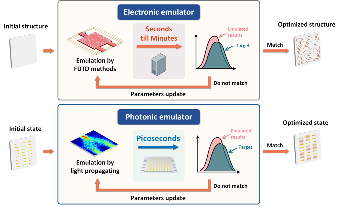
Figure 1. Conceptual drawing of the electronic emulator and the photonic emulator for inverse design.
Researchers led by Prof. Jianji Dong and Prof. Xinliang Zhang in Huazhong University of Science and Technology (HUST), China, have proposed an efficient inverse design strategy, called a photonic emulator, that uses light propagation instead of electromagnetic simulation. This work shows that the concept of propagation-as-computation can be used for inverse design to provide an efficient method for designing reconfigurable integrated photonic devices. The researchers designed a proof-of-principle photonic emulator chip and successfully demonstrated various typical single- and multiwavelength devices and functions, such as an optical multiple-input−multiple-output (MIMO) descrambler (at the modulation rate of 10 Gbit/s), matrix computation (percentage error < 2%), and a tunable wavelength selective switch (extinction ratio > 10 dB for three-wavelength routing). The successful implementation of these typical applications proves the photonic emulator’s viability and great potentials in large-capacity optical communication and large-scale optical computing. The concept of a photonic emulator opens a new avenue for photonic inverse design with the capability of fast and online learning. The photonic emulator breaks the mindset of electromagnetic simulation based on microelectronics hardware and opens a completely new avenue for high-speed and low-energy inverse design by introducing the concept of propagation-as-computation into the field for the first time, thereby making previously unachievable function or higher-performance integrated photonic device design possible in the future. The work entitled Photonic Emulator for Inverse Design was published as a cover article on July 12, 2022 in ACS Photonics.

Figure 2. Design of the photonic emulator. (a) Schematic diagram of the photonic emulator. (b) Microscope image of the photonic emulator chip. (c) Overall photograph of the packaged chip. (d) Thermal distributions of the chip when specific voltages are applied, and the temperature values of the colorbar are in °C. TEC, thermo electric cooler; PCB, printed circuit board.
DOI: https://doi.org/10.1021/acsphotonics.2c00716