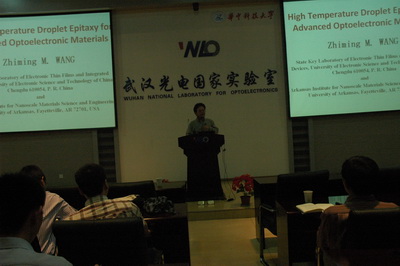
Title:High temperature liquid droplet epitaxial growth of advanced photoelectric materials
Speaker: Prof. Zhiming M. Wang
Time:May. 15. 2012.14:30-15:30
Venue: Room A101 At WNLO
Abstract:
Droplet epitaxy enables fabrication of three-dimensional nanostructures in both lattice-mismatched and lattice-matched materials system. At high temperatures it offers relative high optical and electric properties and also a rich spectrum of nanostructured morphologies such as quantum rings, quantum-dot molecules, and nanoholes. This presentation will focus on recent developments in high temperature droplet epitaxy and presents the challenge and promise of its application in optoelectronic field.
Biography:
Zhiming M. Wang obtained his Ph.D. in condensed matter physics from the institute of semiconductors, Chinese Academy of Sciences Beijing in 1998. He carried out post-doctoral work in molecular-beam epitaxy and scanning tunneling microscope at Paul-Drude-Institute for solid state electronics Berlin (1998-2000), and was a research associate in the physics department of the University of Arkansas (2000-2007) before joining the Arkansas Institute of Nanoscale Materials Science and Engineering in 2007 where he was a Research Professor until June 2011. Now he is a Professor of National 1000-Talent Program, working in the University of Electronic Science and Technology of China, Chengdu. His research has centered on the structural, optical, and electrical properties of low-dimensional semiconductor nanostructures. He has published more than 160 scientific articles in peer reviewed journals and edited several conference proceedings. He serves on the editorial board of the book series “Lecture Notes in Nanoscale Science and Technology” and “Springer Series in Materials Science” as well as being the journal editor-in-chief of “Nanoscale Research Letters”.
