High speed optical communications demand large bandwidth and low power consumption in the future growing data traffic. Optical intensity modulators, as one of the most important devices in converting electric signals to optical ones, ideally need to exhibit the merits of high modulation speed, large bandwidth, small footprint, low loss and ultra-low power consumption. The typical modulators can be achieved by light absorption in waveguide or light interference after phase tuning.
For instance, traditional electro-absorption modulators, like germanium-based modulators, need a reverse bias voltage on a p-i-n-like structure to obtain an imaginary part change of the material’s permittivity, and they are mostly limited by the operation wavelength bandwidth due to their finite band gaps. The light interference type intensity modulators, achieved by controlling the real part of silicon permittivity to generate a phase change are typically designed by micro-ring resonators (MRR) or Mach-Zehnder interferometers (MZI). They require either a precise fabrication method or a large footprint on the chip, which restricts their integration on large scale circuits. To meet the requirement of high-speed and low-energy consumption for the next generation communication systems, a compact integrated electro-optical modulator with a large bandwidth and MD is in desperate.
One of the most effective ways to introduce light-matter interaction is to integrate graphene on silicon devices. As a novel material, graphene has a 2D structure which is a monolayer of carbon atoms formed in honeycomb lattice. Consequently, it performs a unique energy band structure. Due to its special 2D structure, graphene has the merits of easy fabrication in integration, ultra-wide band spectrum, tunable Fermi level as well as high carrier mobility. In the meantime, the van der Waals force between different layers of graphene can also make hybrid integrated devices without ‘lattice mismatch’ problem. To obtain large modulation depth, using membrane-type photonic crystal waveguide (PhCW) with slow light effect is a new way to improve weak light-matter interaction with graphene in nanometer-scale devices.
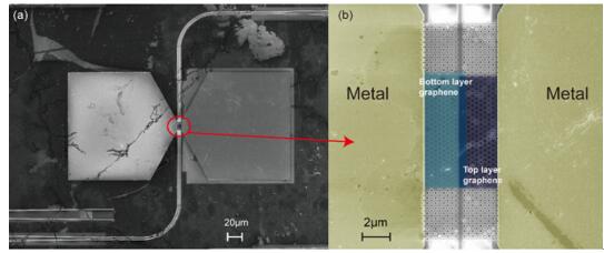
To achieve large modulation depth and bandwidth electro-optical absorption modulator, Professor Jianji Dong from Wuhan National Laboratory for Optoelectronics of Huazhong University of Science and Technology, proposed a graphene-Al2O3-graphene sandwiched stacking on the PhCW structure by combining the merits of PhCW and graphene (shown in Figure 1). Due to the slow light enhancement in the PhCW, a large modulation depth up to 0.5 dB/μm with a bandwidth of 13.6 GHz is theoretically predicted. They successfully fabricated the modulator obtaining a bandwidth of 12 GHz. This design can significantly increase the modulation depth of the modulator without sacrificing the modulation speed. It also removes the doping in the waveguide which greatly simplify the fabrication process. The proposed electro-absorption modulator may have potentials in the optical interconnects or data-center applications.

Figure 1. (a) Schematic structure of the double-layer graphene PhCW modulator. (b) Cross-section of the device with equivalent RC circuit.

Figure 2. (a) SEM image of the modulator. (b) Detailed structure of the active part.
Relevant research results were recently published in Nanophotonics. Professor Jianji Dong and Dr. Yunhong Ding are the corresponding authors. The work was supported by the National Natural Science Foundation of China (61622502, 61805090).
Full text can be viewed by:https://doi.org/10.1515/nanoph-2019-0381
[1] Cheng, Z., Zhu, X., Galili, M., et al. (2019). Double-layer graphene on photonic crystal waveguide electro-absorption modulator with 12 GHz bandwidth. Nanophotonics, doi:10.1515/nanoph-2019-0381.