Ultra-compact, and power-efficient optical modulators are of great importance for on-chip optical interconnects. Graphene has been widely explored to construct compact high-performance optical modulators for its high electron mobility, wide operation bandwidth and electric tunability of conductivity by gating. In recent years, a plenty of graphene modulators have been proposed. However, some of them presented small modulation depth owing to the weak interaction between electric field and the graphene plane, while some other works composed of sophisticated structures that are hard to achieve in experiment. As a result, it is of great value to exploit novel plasmonic structures that not only can achieve high MD, but also can relax the fabrication difficulty.
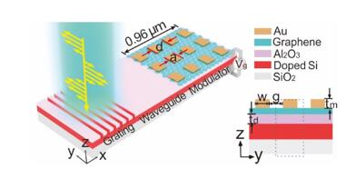
Prof. Lin Chen’s group from Optoelectronic Devices and Integration Division of Wuhan National Lab for Optoelectronics, proposes a novel plasmonic metasurface structure, which is capable of guiding surface plasmons (SPs) with the orientation of the major component of the electric field being parallel to the graphene plane. By properly optimizing the geometries of the metasurfaces, the dispersion relation of SP modes can be well engineered to reduce the group velocity of SP modes. The resultant graphene modulator presents significantly improved MD of 4.66 dB/μm due to the enhanced interaction between the slow SP modes and graphene. Moreover, the one-layer ultra-thin plasmonic metasurface greatly reduces the fabrication difficulty.
This work titled as "Slow light enabled high-modulation-depth graphene modulator with plasmonic metasurfaces " has been recently published in Optics Letters, and also selected as editor’s pick. This work was supported by the National Natural Science Foundation of China (Grant Nos. 11474116, 11674118).

Figure. Schematics of the high-modulation-depth graphene modulator with plasmonic metasurfaces.
Address:
https://www.osapublishing.org/ol/abstract.cfm?uri=ol-44-22-5446