Silicon-on-insulator (SOI) is becoming a powerful and novel platform for photonic integrated circuits (PICs) due to the high integration and the complementary metal oxide semiconductor (CMOS) compatibility. Due to the extremely low luminous efficiency of silicon, external light sources are currently mainly used. However, the extremely small optical components, such as the subwavelength waveguide, present great challenges in the design of fiber-to-chip interfaces. There are two conventional approaches to solve this problem, including edge coupling and vertical coupling. The latter based on diffractive gratings is widely adopted for its flexibility, easy fabrication, large alignment tolerance and so on.
The basic vertical coupling solution is one-dimensional grating coupler (1D GC). Different special designs make the performance of the 1D GC better and better, but there is still an undesirable effect of strong polarization dependence. The proposed two-dimensional grating couplers (2D GCs), which can be regarded as a combination of two orthogonal 1D GCs, make the problem solved. It can decompose different polarization states into two orthogonal polarization states, which are respectively coupled into the waveguide, and simultaneously realize coupling of optical signals, polarization splitting, and polarization rotation.
In order to eliminate the PDL, an active scheme with a phase shifter has been proposed, but it needs extra power consumption. Besides, some special etching patterns have been proposed to reduce PDL, such as diamond patterns, plum patterns and other solutions. Nevertheless, the sharp tips in diamond patterns and plum patterns must be well-shaped in fabrication, or the coupling efficiency will degrade significantly.
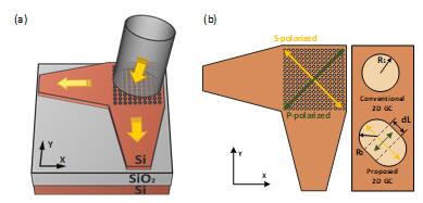
In order to overcome this problem, Professor Dong Jianji from Wuhan National Laboratory for Optoelectronics of Huazhong University of Science and Technology proposed a simple elliptical-like etching pattern, which enables the 2D GC to achieve ultra-low PDL and high manufacturing tolerance. The simple etching pattern consists of two identical semicircles and a rectangle is embedded between them. By adjusting the length of rectangle, the coupling spectrum shift between the S- and P-polarized light is reduced. The 2D GC realizes ultra-low PDL in the C-band and the work provides a technical reference and new ideas for the design of two-dimensional grating couplers.

Fig. 1. (a) Schematic structure of conventional 2D GC. (b) Top view of our proposed 2D GC.
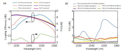
The experimental results show that the coupling efficiency is -4.2dB and the PDL value is 0.2dB in the whole C-band. As shown in Fig. 2, when the semicircular radius and the rectangular length has deviated by ±20 nm from the optimized structure, the 2D GC can still maintain a low PDL in the C-band range. In addition, the elliptical-like etch pattern provides a large feature size of 310 nm, greatly reducing manufacturing difficulties. The design has a good tradeoff between CE, bandwidth and fabrication tolerance.

Fig. 2. (a) Measured coupling efficiency and PDLs of the proposed and conventional 2D GCs. (b) Measured PDLs of 2D GCs with different cell parameters.
Relevant research results were recently published in the journal Optics Express. Professor Dong is the corresponding author. The work was supported by the National Natural Science Foundation of China (61622502, 61805090). Full text can be viewed by
https://www.osapublishing.org/oe/abstract.cfm?uri=oe-27-16-22268
[1] Y. Xue, H. Chen, Y. Bao, J. Dong and X. Zhang, “Two-dimensional silicon photonic grating coupler with low polarization-dependent loss and high tolerance,” Opt. Express, 27, 22268 (2019).