Since the energy consumption and band width limit have restricted the performance of large-scale integration circuit, on-chip optical interconnect has been recognized as a potential solution. Silicon photonics is the most promising platform for integration of photonic and electronic components, however, is limited by the lack of efficient active devices compatible with traditional complementary metal-oxide-semiconductor (CMOS) technology. Ge and SiGe materials draw much attention as the corresponding wavelength of direct bandgap of Ge lies within the communication C-band, while the indirect L-valley band edge is only about 140 meV lower than the direct Γ-valley band edge. Several CMOS compatible schemes have been developed to engineer the band structure of Ge related materials, including Ge/SiGe quantum wells, suspended Ge microstructures, and GeSn alloys. Ge/SiGe quantum wells electro-absorption modulators have shown advantages in aspects of small foot print and low energy consumption. Because of strong quantum confinement, the direct bandgap absorption edge energy of Ge/SiGe quantum well is larger than that of bulk Ge. Although the absorption edge can be shifted by applying different bias voltages, the degeneration of absorption contrast ratio is observed by the experiment. High bias voltage is also not preferable for large-scale integration. The operating wavelengths of theGe/SiGe MQWs modulators are thus limited.
We propose a novel design of Ge/SiGe MQWs zero-biased electro-absorption modulators covering 1380-1550 nm wavelength. By introducing 0.18%-1.6% uniaxial tensile strain, those modulators can be fabricated on the 10 /12 nm Ge/Si0.19Ge0.81MQWs chip. The simulation results show that uniaxial tensile strained Ge/SiGe quantum well has an enhanced TE mode absorption contrast and suppressed TM mode absorption for waveguide configuration.Under 1.6% uniaxial strain, the TE absorption contrast is improved by 3.1 dB for 0V/2V voltage swing while the TM absorption coefficient decreases by two-thirds.The proposed electro-absorption modulator with higher TE mode absorption contrast is benefit to the applications of on-chip optical communications. The improvement in TE absorption makes the device suitable for waveguide integrated highly efficient modulation.
The paper is published on Optical Express (Vol. 25, Issue 10, 2017.doi: 10.1364/OE.25.010874). This work is supported by the National Natural Science Foundation of China under Grant No. 61435004.

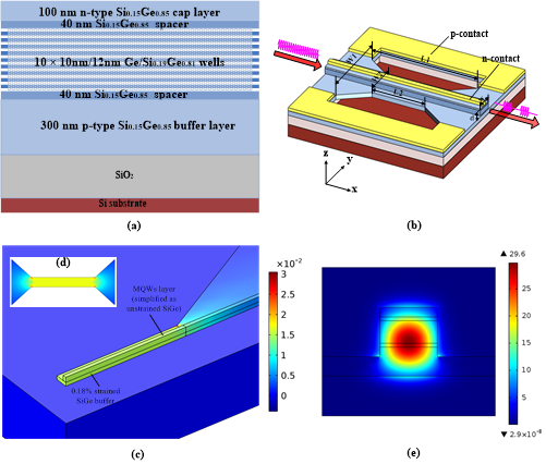
Fig.1.(a) Epitaxy design of the MQWs structure. (b) Schematic of the electro-absorption modulator with suspended microbridge structure. (c) Cross-section map of the strain tensor elementεxxdistribution. W1=165μm, W2=2μm, L1=300μm, L2=20μm. (d)εxxdistribution in the x-y plane with a distance of 150 nm away from the bottom of the buffer layer. (e) Field distribution of the TE field Eyfor the quasi-TE fundamental mode atλ=1550 nm. w=600 nm, d=512 nm.