In Schottky photodetectors (PDs) based on internal photoemission (IPE), the hot carriers created by light absorption in metal/silicide have chance to be emitted over the Schottky barrier and collected in the semiconductor as photocurrent. This type of device can be used in communication and imaging, and provide one of the solutions to all-silicon long-wavelength photodetection in telecommunication bands. With advantage of sufficient light absorption, the waveguide Schottky PDs have bottleneck in performances: 1. the low internal quantum efficiency limits the device responsivity; 2. The plasmonic modes for light absorption should have large mode power attenuations (MPAs) to reduce the device sizes and realize the dark current suppression at room temperature. However, large MPA means high optical confinement in small absorption area, and the large mode field mismatches make it difficult to couple light from free space or photonic mode of dielectric waveguide to the plasmonic mode, and then the absorptance of device is low.
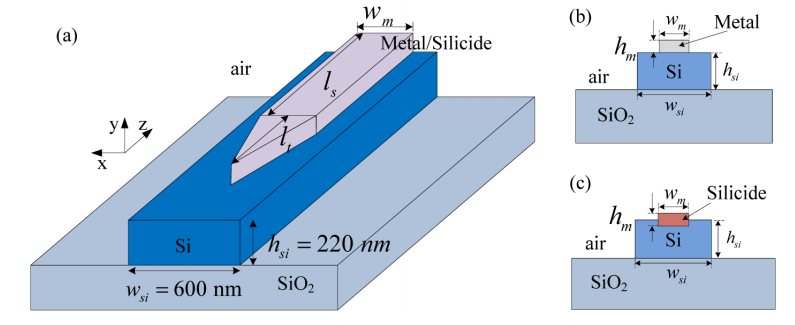
Jingshu Guo and Zhiwei Wu from Optoelectronic Devices and Integration laboratory (OEDI) of Wuhan National Laboratory for Optoelectronics (WNLO),investigate the light absorption enhancement in waveguide Schottky photodetector integrated with ultrathin metal/silicide stripeunder the guidance of Yanli Zhao. The ultrathin metal/silicide (thickness ≤ 10 nm) can enhance theinternal quantum efficiency by utilizing hot carrier reflections between the internal surfaces of absorption area.The plasmonic waveguide proposed by us is constructed by Si nanowire waveguide with ultrathin metal/silicide stripe covered, as Fig. 1 shows. The waveguide cross sections are slightly different between metals and silicides because of different fabrication methods. The silicides are classified to metal-like and non-metal-like in this plasmonic waveguide. The mode hybridization betweenaab0mode and quasi-TE mode are presented when using metal/metal-like silicide. Theaab0-quasi-TE hybrid modes can be coupled from TE photonic mode efficiently, and then absorb light efficiently. In 5 nm Au stripe, a high absorptance of 95.6% (responsivity: 0.146 A/W) is achieved within area of only 0.14 μm2, without using resonance structure. This small contact area helps for getting a low dark current of 8.03 nA at room temperature and a high 3dB bandwidth of 88 GHz. As for nonmetal-like silicide, the plasmonic modes (sabmandaabm)are cut-off, and the mode hybridization mentioned above can not be found. The quasi-TM mode should be used. Using 2 nm PtSi stripe, the optimized responsivity can be up to 0.71 A/W in theory. However, the low absorption ability of quasi-TM mode leads to a long absorption length of 77.7 μm and a large contact area of 3.9 μm2. Both the low Schottky barrier height and large contact area result in a high dark current of 35.9 μA at room temperature. A relatively narrower and thicker silicide strip is better for dark current suppression in this case. We argue that this study can promote the research of waveguide Schottky photodetectors, which has potential to detect light in near infrared bands in integrated Si photonic circuits.
This work "Enhanced light absorption in waveguide Schottky photodetector integrated with ultrathin metal/silicide stripe" has been published on theOptics Express (Vol. 25,No. 9,pp. 10057-10069, 2017).
The study was supported by the Fund Project for Transformation of Scientific and Technological Achievements, Director Fund of Wuhan National Laboratory for Optoelectronics and Huawei Innovation Research Program.

Fig.1. (a) Plasmonic waveguide for light absorption, the waveguide cross sections withcovered ultrathin film of (b) metal and (c) silicide.