On April 30th, Nature Communications published the results of research on non-lead perovskite X-ray imaging by Professor Jiang Tang from Wuhan National Research Center for Optoelectronics and Associate Professor Niu Guangda. The paper is entitled “Heteroepitaxial passivation of Cs2AgBiBr6 wafers with suppressed ionic migration for X-ray imaging".
X-ray detectors are widely used in medical imaging, security screening and product testing. X-ray direct detection based on metal-halogen perovskite can convert X-ray into electric signal in one step, which has the advantages of high sensitivity, low detection limit and high integration. It is widely concerned in the field of radiation detection, and its excellent detection property benefits from its High X-ray attenuation coefficient, long carrier diffusion distance, low temperature preparation and so on. In response to the toxicity of lead-based perovskites, the research team published an X-ray direct detection study based on bismuth silver bismuth bromide (Cs2AgBiBr6) non-lead perovskite single crystal in October 2017 (Nat. Photon 11, 726, 2017). The lead in the lead-based perovskite CsPbBr3 is replaced by silver and antimony to avoid the use of lead, and Cs2AgBiBr6 has a larger ion mobility activation energy than the lead-based perovskite, and the sensitivity of the single crystal-based detector achieved 105 μC Gyair-1cm-2 with a minimum detection limit of 59.7 nGyairs-1.
In order to further realize the application of perovskite-based X-ray imaging, it is still necessary to solve the problem of large-area thick film preparation and ion drift. Due to the difficulty of X-ray focusing (refractive index close to 1), the imaging detector area is required to match the target object. The perovskite polycrystalline thick film is an effective means to achieve large-area preparation. At the same time, the ion drift of perovskite causes baseline drift. The signal output is unstable, the noise is large, etc., which seriously affects the back-end circuit integration and signal processing.
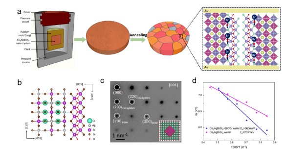
Based on the previous work, the researchers used cold isostatic pressing technology to compress non-lead perovskite Cs2AgBiBr6 polycrystalline powder into a specific size multi-wafer to meet large-area imaging requirements (Figure 1a). At the same time, the lattice mismatch rate of BiOBr and Cs2AgBiBr6 {001} crystal faces is only 1.6%, and the epitaxial matching is high (Fig. 1b). BiOBr can be formed by low temperature hydrolysis of BiBr3, which is helpful for the preparation of epitaxial passivation layer.

Figure 1. (a) Schematic diagram of Cs2AgBiBr6 multi-wafer prepared by cold isostatic pressing; (b) BiOBr and Cs2AgBiBr6 epitaxial relationship model; (c) Selected area electron diffraction and epitaxial growth model; (d) Comparison of ion migration before and after passivation
The researchers milled the Cs2AgBiBr6 crystal into a powder, and used a cold isostatic pressing method to prepare a polycrystalline thick film with controlled area. The subsequent annealing treatment at 350 °C promoted grain boundary fusion. The epitaxial passivation layer of BiOBr is prepared by additionally adding BiBr3 to the raw material to generate BiOBr in situ during subsequent annealing. Selected area electron diffraction confirmed the epitaxial growth relationship between BiOBr and Cs2AgBiBr6 (Fig. 1c). BiOBr can effectively reduce the Br-vacancy defect at the grain boundary of Cs2AgBiBr6, thereby reducing the ion migration caused by Br-vacancy. Both theoretical calculations and experimental results demonstrate the inhibitory effect of BiOBr epitaxial passivation on the ion migration of Cs2AgBiBr6 grain boundary. The activation energy of ion mobility after passivation is increased from 203 meV to 360 meV (Fig. 1d), which is equivalent to the Cs2AgBiBr6 single crystal phase material(348 meV).

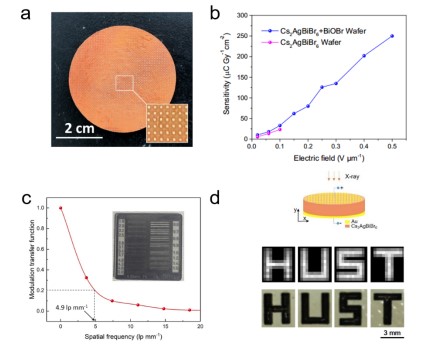
Figure 2. (a) X-ray detector based on Cs2AgBiBr6 multi-wafer; (b) Modulation transfer function (MTF) curve obtained by device edge sensitivity (c) edge-edge test; (d) Imaging process and X Radiography application
The prepared X-ray detector based on Cs2AgBiBr6 wafer (Fig. 2a) has a baseline drift velocity of only 7.4×10⁻⁵ nA cm-1 s-1 V-1, which is two orders of magnitude lower than lead-based perovskite (1.7×10⁻³ nA cm-1 s-1 V-1). The device sensitivity is 250 μC Gy air-1 cm–2@0.5V um-1 (Figure 2b). The modulation transfer function (MTF) of the detector was tested by the edge method (Fig. 2c), and the spatial resolution was 4.9 line pairs/mm corresponding to the 20% MTF value, and the X-ray lattice and line array imaging were initially realized (Figure 2d).
This work provides a method for controlling the preparation of polycrystalline thick films. The innovative strategy of using heteroepitaxial growth to passivate grain boundaries to suppress ion migration is proposed, which provides a new idea for solving the ion migration of perovskites. Future integration with thin-film transistor arrays is needed to achieve the ultimate goal of large-area X-ray imaging and image processing.
The work was completed in cooperation with Prof. Xiangshui Miao, Professor Kanhao Xue and Professor Qingguo Xie from the School of Optical and Electronic Information, and received funding from the Ministry of Science and Technology Key Research and Development Program (2016YFB0700702, 2016YFA0204000) and the National Natural Science Foundation of China (51761145048). Postdoctoral Bo Yang, doctoral students Weicheng Pan, Haodi Wu from Huazhong University of Science and Technology Wuhan Optoelectronics National Research Center are the co-first authors, Professor Tang Jiang and Niu Guangda associate researcher are the co-corresp