Spectrometers play a pivotal role in modern optical applications. The development of miniaturized spectrometers meets the requirements of portability, low cost, small size, and stability for various emerging spectral analysis applications, such as lab-on-a-chip systems, cell detection and analysis, and even spectrometers on mobile devices.
Conventional miniaturized spectrometers are generally obtained by shrinking down the dispersive elements or filters in bulky desktop spectrometers via integrated photonics technology. Computational reconstruction is an emerging method of spectrometer implementation in recent years. This method pre-calibrates the mapping between the incident light and the output channels, and then uses a reconstruction algorithm to iterate with a computer. However, the existing solutions have the disadvantages that they cannot be expanded for various requirements. Besides, the scheme to obtain spectral responses based on material engineering has high complexity in material processing and integration, which brings problems such as high cost.
Professor Jianji Dong et al. in the research group led by Professor Xinliang Zhang from Wuhan National Laboratory for Optoelectronics, Huazhong University of Science and Technology, demonstrated a generalized spectrometer based on nanobeam cavity array and computational reconstruction. By combining a CMOS-compatible nanobeam resonator array with a computational reconstruction algorithm, a spectrometer with compact size, easy scalability and portability is obtained, as shown in Figure 1. The demonstration uses a single nanobeam resonator for a compact wide-spectrum response unit, and the resonant frequency of these nanobeam resonator cavities is finely tuned. The dense arrangement constitutes an array of nanobeams covering the working band. By using such array to detect the incident light, the spectrometer function can be achieved after retrieving the signal with pre-read transmission responses.
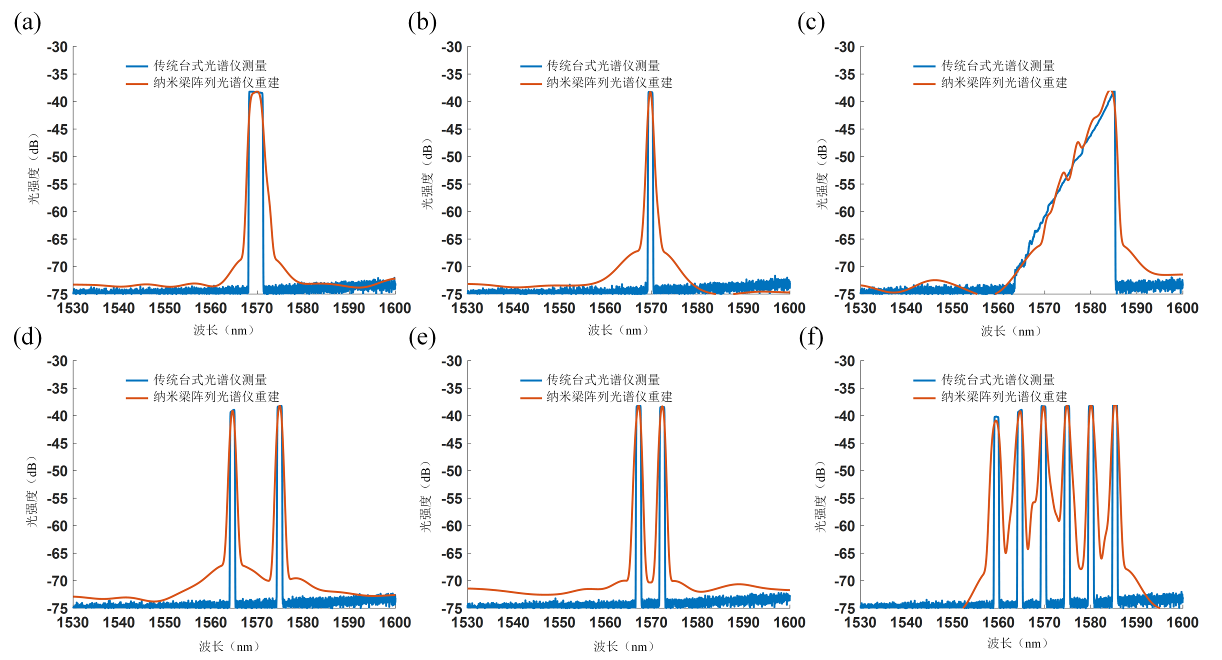
The divice can realize spectral reconstruction up to 30 dB extinction ratio, as shown in Figure 2, for single-peak input with spectral width of 3 nm and 1 nm, double-peak input with interval of 10 nm and 5 nm, as well as triangular and multi-peak input.
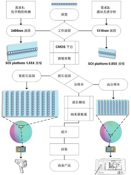
In addition, the nanobeam resonator array spectrometer chip can be flexibly designed and produced according to different product requirements and feedbacks, without incurring excessive costs for redesign and optimization, as shown in Figure 3. For example, the 2400 nm band will use a scaling parameter of 1.55 times, while the 1310 nm band will use a scaling parameter of 0.85 times. After transplanting the working band of the nanobeam resonator, parameters of the nanobeam array can be further determined according to the wavelength range and the resolution. Being a general-purpose spectrometer chip that can be quickly customized, the nanobeam spectrometer shows great potential to be developed as a commercial product for various applications, thus possessing a unique advantage in practicality compared to other spectrometer solutions.

Fig. 1. Operational schematic and characterization of the PCNC array spectrometer. (a) Receiving and response process of the PCNC spectrometer to arbitrary spectrum incident-light: schematic incident process (top), transmitted intensities (middle), and transmission functions (bottom). (b) Computational reconstruction process. Mathematical description of the receiving and the response process of the PCNC spectrometer (bottom), solving method for the equation set (middle), and reconstructed spectrum of the incident light (top). (c) SEM image of the fabricated PCNC spectrometer SOI chip. There is only a 3 μm distance between each PCNC unit. Scale bar: 2 μm. (d) Normalized spectral transmission of each filter unit in the PCNC spectrometer.

Fig. 2. Incident spectra measured by a conventional benchtop spectrometer and computational reconstruction with the PCNC spectrometer as blue and red lines, respectively. (a) 3 nm FWHM single peak spectrum of the incident light. (b) 1 nm FWHM single peak spectrum of the incident light. (c) Broadband incident light with triangular spectrum. (d) Two-peak spectrum of incident light with 10 nm distance. (e) Two-peak spectrum of incident light with 5 nm distance. (f) Broadband incident light with a range of spectral peaks. FWHM: full width at half maximum.

Fig. 3. Standard customization flow from proposed PCNC prototype to commercial miniaturized spectrometers. Two types of application demands: chemical gas characterization and telecom spectrum analysis as examples
Relevant research results were recently published in ACS Photonics. Full text can be referred by: https://doi.org/10.1021/acsphotonics.1c00719.
Written by: Dong Jianji
Reviewed by: Dong Jianji, Gou Bingbing