With growing demand for capacity in the big data era, advanced modulation formats and multi-dimensional multiplexing technologies have been widely used in optical communication system,which can effectively increase data transmission capacity and spectral efficiency. Demultiplexing and demodulation of multiplexing signal carrying advanced modulation format is significant for high-speed on-chip optical interconnection. Currently, photonic integrated function devices are advancing concomitantly towards miniaturization. Different from electronic chips with the ability of ultra-dense integration, optical function devices such as mode (de)multiplexer, 90° optical hybrid, crossing, etc., share a size usually up to dozens or even hundreds of micrometers, resulting in optical modules that have large footprints of up to several millimeters,which severely limits their large-scale integration ability and increases the cost of optical modules.
In recent years, research progress suggests that the superminiature size of inverse-designed on-chip dielectric metasurfaces can promote the dense integration of photonic devices or modules. Although inverse-designed method can realize ultra-compact optical devices, there are still no reports on higher order mode (de)multiplexer (such as four-mode (de)multiplexer) and optical hybrid, which are the core components of future multimode coherent optical communication system with higher capacity.

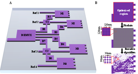
Figure 1. Schematic diagram of the ultra-densely integrated multi-dimensional photonic chip
On January 31th, 2022, Laser and Photonics Reviews online published a research paper on an ultra-densely integrated multi-dimensional photonic chip titled Dielectric metasurfaces enabled ultradensely integrated multi-dimensional optical system, which was accomplished by Prof. Zhang Xinliang and Prof.Dong Jianji’s team from Huazhong University of Science and Technology, in cooperation with several researchers from the Hong Kong Polytechnic University.
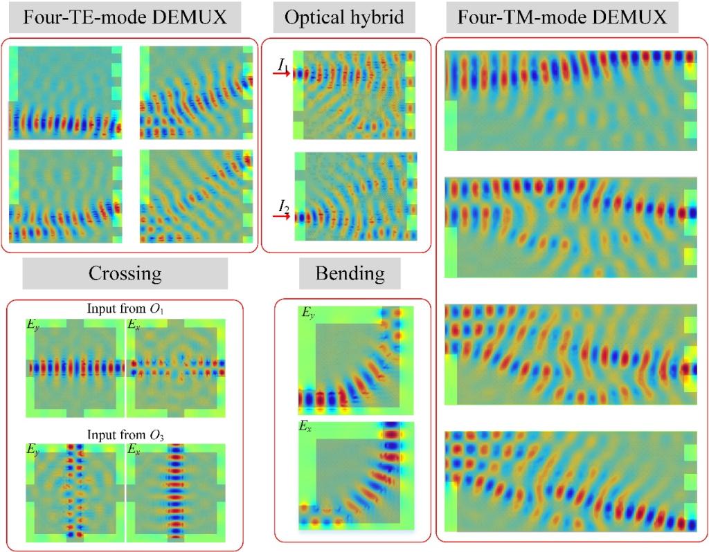
In order to effectively reduce the volume of optical modules, it is necessary to reduce the size of basic functional components. Based on the inverse-designed method, five ultra-compact on-chip dielectric metasurface functional devices are successfully designed, includingfour-TE/TM-mode demultiplexer (4.8×4.8 μm2and 9×4 μm2), optical hybrid (4.8×4.2 μm2), crossing (3.6×3.6 μm2) and bending (2.4×2.4 μm2). Figure 2 shows the simulated propagation field of the five optical devices, indicating that these devices can perform their corresponding functions well. These devices have feature sizes of only several microns, which is more than one order of magnitude smaller than that of the traditional works. Inverse design provides a powerful method for the miniaturization of photonic devices.

Figure 2. Simulation structures of the inverse-designed devices
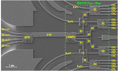
Subsequently, an ultra-densely integrated photonic chip, namely four-mode demultiplexing optical hybrid (MDOH), is proposed based on these fundamental devices. A mode demultiplexer is first used to sort the four input TE modes from the bus waveguides. Then multiple bendings (B1-B8) further separate the four beams, and each beam is injected into an optical hybrid (H1-H4). Then, two crossings (C1-C2) assist to lead out the reference waveguides (Ref1-Ref4) of optical hybrids. In practice, local light is injected from the reference waveguides. Based on the light intensity in the four output ports of each optical hybrid, advanced modulation formats carrying on the four modes can be demodulated independently. Thus, the complex optical modules or subsystems with small areas can be assembled after the basic components are demonstrated. In this work, 15 functional devices are integrated within an area of only 20×30 μm2. It confirms the possibility of ultra-compact multi-dimensional optical systems, greatly expands the application of on-chip metasurface integrated devices, and paves another way for large-scale high-capacity optical communication systems. In the future, it can be further combined with wavelength division multiplexing or polarization division multiplexing to achieve more densely integrated optical signal processors.This work also promotes the development of large-scale and ultra-densely integrated single-chip microprocessors.

Figure 3. Scanning electron microscopy image of the multi-dimensional photonic chip
This research finding is published online in Laser and Photonics ReviewstitledDielectric Metasurfaces Enabled Ultradensely Integrated Multidimensional Optical System. Prof. Dong Jianji from Huazhong University of Science and Technology is the corresponding author. Associate Prof. Zhou Hailong and postdoctoral fellow Wang Yilun are the co-first authors. Co-authors include Prof. Ping-kong Alexander Wai, Dr. Li Feng, Dr. Huang Dongmei from Hong Kong Polytechnic University, and Dr. Gao Xiaoyan, Prof. Gao Dingshan and Prof. Zhang Xinliang from Huazhong University of Science and Technology.
Paper link: https://onlinelibrary.wiley.com/doi/10.1002/lpor.202100521
Written by: Dong Jianji
Reviewed by: Gou Bingbing