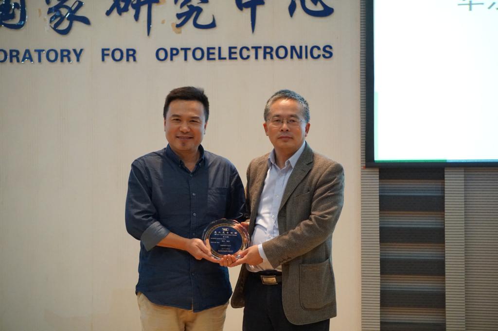
Wuhan Optoelectronics Forum No. 171 was successfully held in Auditorium A101 at Wuhan National Laboratory for Optoelectronics (WNLO) in the afternoon of November 12. Professor Ya Cheng from East China Normal University and Shanghai Institute of Optics and Mechanics delivered an exciting presentation entitled "Lithium Niobate Photonic Chip". Professor Wei Xiong, from WNLO chaired the forum. Professor Lu Peixiang, the vice director of WNLO, awarded the forum medal to Professor Ya Cheng.
Professor Cheng pointed out that the brilliance of Silicon Valley comes from integrated circuit technology. From the first electronic computer in 1946 to the current smart electronic products, the computing power has been increasing. But there are still many problems just like too slow computing speed, too low energy efficiency, opto-electronics change frequently etc. The current solution is to use high-speed, high-capacity, high-efficiency large-scale photonic integration to break through the bottleneck of electronic integration, and it will be used in big data, high-speed communications, lidar, biochemical sensing and other fields. Photonic integrated materials need to have three characteristics: 1. Ultra-low transmission loss, 2. Ultra-small turning radius, 3. Ultra-fast phase adjustment, and Lithium Niobate has a significant advantage among many materials.
Firstly, the report introduced the production of the Lithium Niobate Micro-disk withQ>105by femtosecond laser etching of Lithium Niobate and then etching with a focused ion beam. But to make higher-quality photonic structures, ion beametchingis far from enough. Professor Cheng pointed out that the preparation of macroscopic optical systems relies on optical polishing, while the preparation of integrated optical systems generally relies on ion etching. Professor Cheng used polishing equipment to break through the loss bottleneck of integrated optical devices. Firstly, a chromium film is deposited on the Lithium Niobate and patterned by femtosecond laser etching, then the Lithium Niobate is patterned by polishing, and finally the silicon dioxide layer and the chromium layer are removed by chemical wet etching. The quality factor of the ring cavity prepared by chemical mechanical polishing can reach the order of107, and the photomechanical, optical comb and high-efficiency nonlinear effects can be clearly observed.
Next, Professor Cheng briefly introduced Lithium Niobate integrated photonic devices from waveguide beam splitters and waveguide couplers to on-chip optical switches, on-chip optical interferometers, and meter-level waveguide delay lines. At the end of the presentation, Professor Cheng summarized the current and future urgent problems and possible solutions of Lithium Niobate integrated photonics technology.
After Professor Cheng finished speaking, he had an enthusiastic academic exchange with teachers and students. Professor Cheng pointed out that there is still room for improvement in silicon-based photonic integration, but the inherent properties of silicon will become a disadvantage. After the manufacturing cost is gradually reduced, the future of Lithium Niobate photonic chip is bright. Amid the warm applause of teachers and students, the report ended.